What a silicon interposer is — the 'bridge board' under AI chips, and why CoWoS became the bottleneck
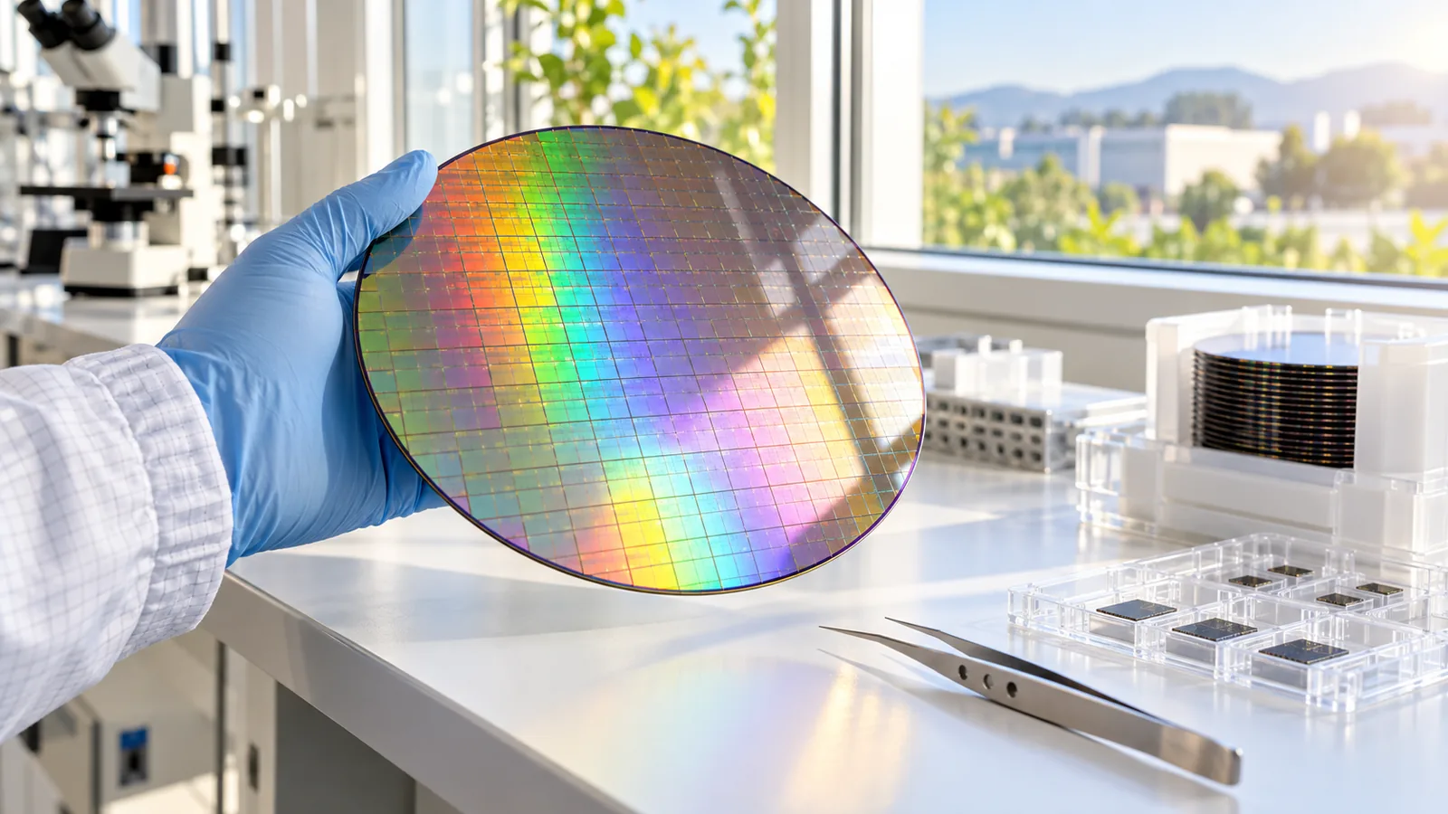
A silicon interposer is a thin slab of silicon that connects AI processors (such as GPUs) with high-bandwidth memory (HBM) inside a single package. The chips sit side by side on top of it, fine wiring patterned inside the interposer links them with thousands of connections, and through-silicon vias (TSVs) carry signals down to the package substrate. Each HBM stack has a 1,024-bit data interface (2,048 bits for HBM4), too dense for an ordinary organic substrate to route, so nearly every HBM-based AI accelerator uses an interposer or a silicon bridge. TSMC's CoWoS packaging is built this way, and demand beyond its capacity has made it a bottleneck for AI chip supply
The three lines
- Definition — thin silicon under the chips: fine wiring between dies on top, TSVs to the substrate below
- Why needed — each HBM stack has 1,024–2,048 data lines; ordinary substrates can't route that
- CoWoS — TSMC's three variants (S, L, R); capacity decides how many AI chips ship
Key questions
- What is an interposer
- **An intermediate layer that connects chip to chip and chip to substrate.** | Layer | Role | |---|---| | Top | Dies such as GPU and HBM | | Micro-bumps | Tiny contacts joining dies to the interposer | | **Interposer** | Fine die-to-die wiring + through-silicon vias (TSVs) | | Substrate | Supports the interposer and connects to the board | | Board | Server motherboard |
- What is CoWoS
- **TSMC's 2.5D packaging: Chip on Wafer on Substrate.** | Variant | Intermediate layer | Feature | |---|---|---| | CoWoS-S | Monolithic silicon interposer | Oldest, densest wiring | | CoWoS-L | Organic layer + local silicon bridges (LSI) | Larger packages; latest big AI chips | | CoWoS-R | Organic redistribution layer (RDL) | Cheaper, lower wiring density |
- Interposer vs silicon bridge
- **An interposer spans the whole package; a bridge is a small piece only where dies meet.** | Item | Silicon interposer | Silicon bridge | |---|---|---| | Size | Large slab under all dies | Small piece under die edges | | Cost | High | Lower | | Size limit | Must stitch beyond one lithography field | Easier to scale package size | | Examples | CoWoS-S | CoWoS-L, Intel EMIB |
A silicon interposer is a thin slab of silicon that connects AI processors and high-bandwidth memory (HBM) inside one package. A GPU and several HBM stacks sit side by side on it, and fine wiring patterned into the slab links them with thousands of connections. It is normally an invisible part, but it made headlines on October 8, 2026, when GlobalFoundries signed a five-year, $2 billion deal to make interposers for TSMC ("GlobalFoundries–TSMC $2 billion interposer deal"). The reason AI chips are scarce lies not only in the fabs that etch them but in the process that lays down this layer and assembles the package.
1. Structure — a middle layer under the chips, above the substrate
| Layer (top to bottom) | What it is | What it does |
|---|---|---|
| Dies | GPU, HBM stacks | Compute and store data |
| Micro-bumps | Solder contacts tens of micrometres across | Attach dies to the interposer |
| Interposer | Thin silicon slab | Top: die-to-die wiring / Bottom: vertical connections via through-silicon vias (TSVs) |
| Package substrate | Organic laminate | Supports the interposer and connects to the server board |
An interposer has no (or very few) computing transistors. Its job is wiring — but wiring so fine it must be drawn with semiconductor lithography. That is why foundries such as TSMC and GlobalFoundries make them. GF's interposers will also carry deep trench capacitors to deliver steady power right next to the chips.
2. Why it's needed — HBM's lane count outgrew the substrate
| Comparison | Standard memory (DDR5 module) | HBM3 stack | HBM4 stack |
|---|---|---|---|
| Data width | 64 bits (2 × 32-bit channels) | 1,024 bits | 2,048 bits |
| Distance to processor | Several cm across the board | A few mm, same package | A few mm, same package |
| Connection | Board traces | Interposer or bridge | Interposer or bridge |
One AI accelerator carries several HBM stacks. Add 1,024–2,048 data lines per stack to power and control lines, and tens of thousands of connections crowd into a few millimetres beside the processor. Organic substrate wiring pitches cannot reach that density; it takes semiconductor processing on silicon. The Register noted that nearly every HBM chip relies on an interposer or silicon bridge.
3. CoWoS — three variants and the bottleneck
CoWoS stands for Chip on Wafer on Substrate. Dies are first bonded onto an interposer wafer, and that assembly is then mounted on a substrate. It is called 2.5D packaging to distinguish it from true 3D stacking.
| Variant | Intermediate layer | Strength | Limit |
|---|---|---|---|
| CoWoS-S | Monolithic silicon interposer | Highest wiring density, proven | Costly as it grows; beyond one lithography field it must be stitched |
| CoWoS-L | Organic layer + local silicon bridges (LSI) | Suits large packages — latest big AI chips | Complex process |
| CoWoS-R | Organic redistribution layer (RDL) | Lower cost | Lower wiring density |
Bottlenecks arise in three places: ① interposer wafer capacity, ② die-to-wafer assembly capacity and ③ final testing. With AI chip demand above that capacity, TSMC is handing parts of the process to outside firms such as Amkor and GF.
4. Competing technologies and what remains
| Technology | Company | Approach |
|---|---|---|
| CoWoS-S / L / R | TSMC | Interposer, bridge, redistribution layer |
| EMIB | Intel | Small silicon bridge embedded in the substrate |
| Foveros | Intel | 3D stacking of dies |
| I-Cube / X-Cube | Samsung Electronics | 2.5D interposer / 3D stacking |
- Glass substrates: Research into glass instead of silicon for the middle layer continues; commercial timing is not set.
- US production: GF Malta volume production is due in the first half of 2028 and TSMC's Arizona packaging in 2029. Until then, most US-made AI chips are packaged in Taiwan.
- Undisclosed numbers: TSMC does not publish monthly CoWoS capacity, and market estimates vary widely.
Sources
- TSMC — CoWoS advanced packaging (3DFabric)
- The Register — TSMC taps GlobalFoundries to bolster US silicon interposer production in $2B deal
- Converge Digest — GlobalFoundries signs $2B TSMC deal for CoWoS interposer manufacturing
- JEDEC — High Bandwidth Memory (HBM) DRAM standards
- Verdict — GlobalFoundries and TSMC agree on $2bn US silicon interposer supply deal