What is co-packaged optics (CPO)? Linking chips with light — half the power, a tenth of the latency
Co-packaged optics (CPO) puts the optical engine — the part that turns electrical signals into light — inside the same package as a network switch or AI chip. Today that job is done by pluggable transceivers at the front of the server, and signals lose power and time travelling across centimeters of copper on the board to reach them. CPO removes that stretch; TSMC claims twice the power efficiency and a tenth of the latency of pluggables. TSMC said in April 2026 its COUPE platform would enter production in the second half of 2026, with network switches from Nvidia and Broadcom first. Samsung Foundry targets optical engines in 2027 and turnkey CPO in 2029.
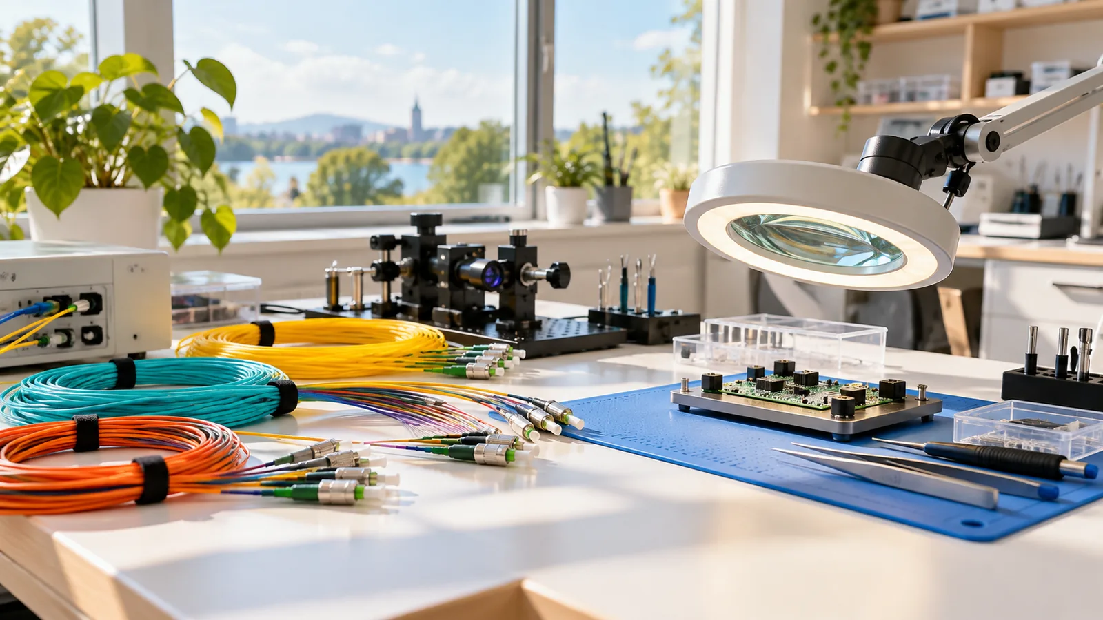
The three lines
- Definition — optical engine in the same package as the chip, replacing pluggable transceivers and the copper in between
- Benefit — TSMC claims 2x power efficiency and 1/10 latency, targeting AI data-center power and heat limits
- Timeline — TSMC COUPE in 2H 2026 with switches first; Samsung optical engines 2027, turnkey CPO 2029
Key questions
- Co-packaged optics meaning
- **The optical engine moves into the chip package instead of a plug-in module at the board edge.** | | Pluggable (today) | CPO | |---|---|---| | Where light conversion happens | Front-panel module | Inside the chip package | | Copper path | Several cm on the board | Millimeters | | Power | Baseline | About half (TSMC claim) | | Latency | Baseline | About 1/10 (TSMC claim) | | Repair | Swap the module | Replace the package |
- When will co-packaged optics be in production
- **TSMC targets 2H 2026; Samsung plans 2027-2029.** | Company | Timing | Detail | |---|---|---| | TSMC | 2H 2026 | COUPE-on-substrate (April symposium) | | Nvidia | 2026 | Quantum-X Photonics InfiniBand switch | | Broadcom | 2026 | Tomahawk CPO Ethernet switch | | Samsung Foundry | 2027 / 2029 | Optical engines / turnkey CPO |
- CPO vs silicon photonics
- **Silicon photonics is how the optical parts are made; CPO is where they are placed.** | Term | Meaning | Relation | |---|---|---| | Silicon photonics | Building optical devices with chip processes | Material/process | | Optical engine | Bundle that converts electrical ↔ light | Made with silicon photonics | | CPO | Optical engine integrated in the chip package | Packaging approach | | COUPE | TSMC's optical engine platform for CPO | Brand |
The next bottleneck in AI data centers isn't the chip — it's the wire between chips. Training clusters stitch tens of thousands of GPUs into one machine, which requires enormous chip-to-chip bandwidth. Long distances already run over fiber, but the short hop from the chip to the optical module is still copper on a circuit board. Power and time leak in those few centimeters. CPO removes them.
TSMC reported a record Q3 on October 15, with 79% of revenue from 7nm-and-below nodes. Connecting those chips is the next arena.
1. How chips connect today
| Step | Pluggable today | CPO |
|---|---|---|
| ① Chip | Switch/GPU outputs electrical signal | Same |
| ② To conversion | Centimeters of board copper to the front panel | Millimeters inside the package |
| ③ Conversion | Plug-in transceiver module | Optical engine beside the chip |
| ④ Transport | Fiber | Fiber |
| Weakness | Signal loss on copper → power spent on correction | Package-level replacement; hard to manufacture |
As data rates rise, signals fade faster over copper. Compensating takes power-hungry circuitry, and that power becomes heat — not trivial when single data-center campuses need gigawatts.
2. What CPO improves
| Item | Effect | Basis |
|---|---|---|
| Power | About half of pluggables | TSMC COUPE claim (2x efficiency) |
| Latency | About 1/10 | TSMC claim |
| Density | More links per area | No front-panel module limit |
| Key device | 200Gbps micro-ring modulator | TSMC |
| Build | Electrical die stacked on photonic die (SoIC bonding) | TSMC COUPE |
3. Who ships what, when
| Company | Product/plan | Timing |
|---|---|---|
| TSMC | COUPE-on-substrate CPO | 2H 2026 (April 22 North America Technology Symposium) |
| Nvidia | Quantum-X Photonics InfiniBand switch (144×800G) | 2026 |
| Broadcom | Tomahawk CPO Ethernet switch (51.2T) | 2026 |
| Samsung Foundry | Silicon photonics PDK (entry announced March 2026) → optical engines → turnkey CPO | 2027 / 2029 |
| Samsung Electro-Mechanics, LG Innotek | Testing CPO substrate samples | Ongoing (TrendForce) |
The first wave in 2026 is network switches, not GPUs. Optical links on GPUs themselves come later. Much of 2026 CPO assembly capacity sits in TSMC's CoWoS advanced-packaging lines — the same lines already busy attaching HBM to AI GPUs.
4. Why it's still hard
| Hurdle | Detail |
|---|---|
| Fiber alignment | Fibers thinner than a hair must be aligned precisely; curing adhesive can shift them |
| Wafer testing | Electrical and optical performance must be tested together |
| Serviceability | Pluggables swap out; CPO means replacing the package |
| Substrates | Large ABF substrate supply is tight; Nvidia may lock in long-term capacity |
A TSMC advanced-packaging director said breakthroughs in wafer testing, fiber-array assembly and high-speed optical packaging will decide how fast CPO scales.
5. What remains open
- Production start: whether TSMC's 2H 2026 ramp has begun is unconfirmed.
- Performance claims: 2x power, 1/10 latency are TSMC's figures.
- Samsung timing: 2028 vs 2029 in different reports.
Sources
- TrendForce — TSMC Targets 2H26 COUPE on Substrate; NVIDIA Could Eye Long-Term Substrate Deals Amid CPO Push
- Design & Reuse — Silicon Photonics Race Intensifies as TSMC Targets 2026 COUPE Production, Samsung Eyes 2029 CPO Turnkey
- LEDinside — Samsung Foundry Reportedly Wins Optical Module Order, Steps Up Silicon Photonics and CPO Drive
- Inside Deep Tech — Co-Packaged Optics: A Full Guide to CPO vs LPO (2026)